SymbiFlow Architecture Definitions
*Warning: This project is a work in progress and many items may be broken.*
This project contains documentation of various FPGA architectures, it is currently concentrating on;
- Lattice iCE40
- Artix 7
The aim is to include useful documentation (both human and machine readable) on the primitives and routing infrastructure for these architectures. We hope this enables growth in the open source FPGA tools space.
The project includes;
- Black box part definitions
- Verilog simulations
- Verilog To Routing architecture definitions
- Documentation for humans
Contents
Getting Started with SymbiFlow Toolchain development
Warning
This documentation explains the first steps in the development of the toolchain itself. If you are looking for the user documentation, please look at https://symbiflow-examples.readthedocs.io/en/latest/ instead.
This section provides an introduction on how to get started with the development of the SymbiFlow toolchain. In order to generate a bitstream (or any intermediate file format), you can use one of the toolchain tests. The following steps describe the whole process:
Clone repository
git clone https://github.com/SymbiFlow/symbiflow-arch-defs.git
Prepare environment
Download all the necessary packages, tools and databases into an isolated conda environment:
cd symbiflow-arch-defs
make env
This also checks out all the submodules and generates the build system (Make or Ninja) from the CMake configuration.
If you want to use the Ninja build tool add this line before calling make env:
export CMAKE_FLAGS="-GNinja"
Build example
While different architectures provide different build targets, there are some targets that should exist for all architectures.
Each architecture has its own toolchain backend that will be called during build. (See Project X-Ray and Project Trellis for more information)
For development purposes a set of test designs are included for each supported architecture. In order to perform a build
of a test design with the Make build system enter the appropriate test build directory specific to your target architecture
and invoke desired make target.
Assuming that you would like to generate the bitstream .bit file with the counter example for the Arty board, which uses Xilinx Artix-7 FPGA,
you will execute the following:
cd build/xc/xc7/tests/counter
make counter_arty_bit
If you use Ninja then the target is accessible from root build directory:
cd build
ninja counter_arty_bit
Note
Test design targets names are based on the following naming convention: <design>_<platform>_<target_step>, where <target_step> is the actual step to be done, e.g.: bit, place, route, prog.
Warning
Generating architecture files is expected to take a long time to build, even on fast machines.
Load bitstream
The last step is to load the bitstream to your platform.
The final output file can be found in the appropriate test directory, i.e:
build/xc/xc7/tests/counter/counter_arty/artix7-xc7a50t-arty-swbut-roi-virt-xc7a50t-arty-swbut-test/top.bit
For every board the loading process may be different and different tools will be required.
OpenOCD is the most widely used tool for loading bitstream in the Symbiflow Toolchain. It is provided as a conda
package during the environment setup and CMake keeps track of its executable. Other programming tools used in Symbiflow that are automatically downloaded and referenced by CMake are tinyfpgab and tinyprog.
For convenience the prog targets are provided for loading the bitstream, e.g.:
make counter_arty_prog
or for Ninja:
ninja counter_arty_prog
Note
Loading the bitstream into an FPGA can be done outside of the Symbiflow. There are multiple tools for loading bitstreams into FPGA development boards. Typically, each tool supports a specific target family or the lines of products of a vendor. Some of the most known are listed in hdl/constraints/prog
OpenFPGALoader
OpenFPGALoader is an universal utility for programming the FPGA devices that is a great alternative to OpenOCD. It supports many different boards with FPGAs based on the architectures including xc7, ECP5, iCE40 and many more. It can utilize a variety of the programming adapters based on JTAG, DAP interface, ORBTrace, DFU and FTDI chips.
Installing OpenFPGALoader
OpenFPGALoader is available in several packaging solutions. It can be installed with distribution specific package managers on Arch Linux and Fedora. There are also prebuilt packages available in conda or packages in tool repository. OpenFPGALoader can also be built from sources. For installation guidelines using both prebuilt packages and building from source please refer to instructions in readme.
Usage
For programming the FPGA use one of these commands:
openFPGALoader -b <board> <bitstream> # (e.g. arty)
openFPGALoader -c <cable> <bitstream> # (e.g. digilent)
openFPGALoader -d <device> <bitstream> # (e.g. /dev/ttyUSB0)
You can also list the supported boards, cables and fpgas:
openFPGALoader --list-boards
openFPGALoader --list-cables
openFPGALoader --list-fpga
If you encounter any issues, please refer to the OpenFPGALoader README as it provides more useful information on the usage of the tool.
Project X-Ray
This section contains the information about the methods and tools used for managing Project-XRay data inside the Architecture Definitions Project.
Flow Diagram
This diagram depicts the most important files in the Architecture Definition project related to Project X-Ray.
Rectangular boxes represent the files within the project, whereas rounded blocks represent the program. Colores indicates either third-party project or projects related to SymbiFlow Toolchain. A detailed description is presented on the figure.

VPR routing graph
Database Contents
This section will describe the prjxray database contents with respect to the routing graph.
Grid
Project X-Ray documents one or more parts. Within a part is a grid.
The grid is documented in tilegrid.json and can be accessed via the
prjxray API via the prjxray.db.Database.grid method.
Each location within the grid is a tile, which has a tile type and grid coordinate. Each instance of a tile type has the same sites, tile wires, and pips. A tile type may have zero or more sites, zero or more tile wires and zero or more pips. Pips are programmable interconnect points, and connect two tile wires together in a programmatic fashion.
A tile may also have a bits definition if the output bitstream configures this tile. A bits definition consists of a block type, a base address, the number of frames in the base address column, a word offset, and a number of words.
Routing fabric
| From | To |
|---|---|
| Local Tile Wire | PIP |
| Local Tile Wire | Site Pin |
| Local Tile Wire | Remote Tile Wire |
| Remote Tile Wire | Local Tile Wire |
| Site Pin | Local Tile Wire |
| PIP | Local Tile Wire |
| Property | Valid choices |
|---|---|
| connections |
|
| Property | Valid choices |
|---|---|
| src_wire | Local Tile Wire |
| dst_wire | Local Tile Wire |
| is_directional | True or False |

A 7-Series part contains nodes, which consist of tile wires. Tile wires are sourced either from a site pin or a pip or a tile wire from another tile within the grid. Tile wires sink to either a site pin or a pip or a tile wire in another tile within the grid. Tile wires have not been observed to have a source and sink that are both site pins.
Tile wires that source or sink within a tile are documented in the
tile type definition, which is found in the tile_type_<tile
type>.json files. The tile type definition has a list of the tile
wires within the tile, a list of pips and a list of sites. If
the tile wires source or sink within the tile, then the tile
wire will appear in either a pip or a site definition. Tile
type definitions can be retrieved via db.Database.get_tile_type method.
All pip definitions have a src_wire and dst_wire keys, indicating what tile wire is connected to each end of the pip.
Note
A bidirectional pip will have the is_directional key set to “0”, but use src_wire and dst_wire as if it was a unidirectional pip.
Each site definition will have a site_type and dictionary of
site_pins, along with site naming information. The site_pins
dictionary maps the site_pin of the site_type to the
tile_wires within the tile. The direction of site_pin can be
found in the site_type definition, site_type_<site type>.json
file. Site type definitions can be retrieved via
db.Database.get_site_type method.
The tile wires combined with the tile’s pip list and the
site_pins definition for each site completes the routing description
for the tile. However there needs to be a relationship between tile
wires from tiles to each other. This is defined in the
tileconn.json file, provides a list of which tile wires are
connected between tiles. The tileconn.json relates tile types via
their grid coordinates.
{
"grid_deltas": [
0,
1
],
"tile_types": [
"CLBLL_L",
"CLBLL_L"
],
"wire_pairs": [
[
"CLBLL_LL_CIN",
"CLBLL_LL_COUT_N"
],
[
"CLBLL_L_CIN",
"CLBLL_L_COUT_N"
]
]
},
This reads as “a CLBLL_L that is at (x+0, y+1) from another CLBLL_L,
- Connect
CLBLL_L(x, y+1).CLBLL_LL_COUT_NtoCLBLL_L(x, y).CLBLL_LL_CIN- Connect
CLBLL_L(x, y+1).CLBLL_L_COUT_NtoCLBLL_L(x, y).CLBLL_L_CIN
The tile wire connections can be retrieved via
db.Database.get_connections.
The tile wire connections from tileconn.json, and the pips and
site pins from each tile_type_<tile type>.json provides a complete
routing graph description for a part between sites. Routing
within sites is done via pb_type architectural XML, and is not
documented as part of prjxray at this time.
VPR routing description
The previous section documented the contents of the prjxray database. Prior to describing the process of converting that database into VPR, a short discussion of the VPR routing data structures is required.
At the most basic level, VPR’s routing graph is made of nodes and edges. Edges are either configurable or static connections between nodes. Static connections are always present. Configurable connections are selected during routing. All edges must have a switch. A switch is used to describe timing information along the edge, and it determines if the switch is configurable or not. The two most common types of switches are SHORT (electrical short) and MUX.
SHORT is used to join two nodes in the routing graph, both logically and for timing purposes. SHORT’s are not configurable.
MUX is roughly equivalent to a pip. It is configurable and is used by the router. For the purposes of timing, the timing on nodes on each side of the pip are seperate. A PASS_GATE is a switch that does not do this isolation.
The detiled description about switch types can be found in VTR documentation .

So edges connect nodes together, but what are the nodes themselves? Nodes are either a source/sink (e.g. a site pin) or are routing fabric. VPR models each source or sink as 2 or more nodes. The site pin is a SINK or SOURCE. To accommodate the idea that a site pin might have multiple routing paths, the SINK or SOURCE then is connected to a IPIN or OPIN respectively. Then IPIN’s/OPIN’s are connected to other nodes. So by default, all IPIN’s connect to exactly one SINK, and all SOURCE’s connect to exactly one OPIN.
There are two routing fabric node types, CHANX and CHANY. CHANX are wires that traverse in the x-direction and CHANY are wires that traverse in the y-direction. Channels lies between tiles (see this image from the VPR routing graph description documentation). Channels cannot extended to the first or last column in the grid.
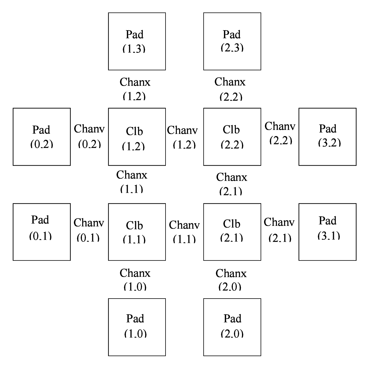
IPIN’s and OPIN’s have a direction that they point in relative to the tile they belong too. They can be on the north, east, west, south, or some combination. For example, in the image above, a pin at (1, 2) on the east side could connect to CHANY nodes at (1,2).
Creating a 7-series routing graph for VPR
In order to create a routing graph for VPR, several new things must be defined:
How to map the routing tile wires into VPR channels or other constructs?
Which side of the tile should site pins be assigned to connect to other tiles (in the case of direct connections like carry chains) and to VPR channels?
After the preparation work, output can be generated for VPR. 3 types of output are generated:
Tile pb_types XML’s that connect site pb_types site pins to tile wires
Architecture XML that is the grid and has direct inter-tile connections
Final routing graph XML
Click on the figure below to zoom-in:

Tile wire classification
Before channels can be formed, tile wires need to be bucketed into their purpose.
The first step is to first re-form nodes that contain all the directly connected tiles wires These nodes are not VPR nodes, they are simply the collection of tile wires that are already a net (electrically equivalent).
Each node then needs to be classified. The simplest classification is a channel wire, which means that pips route on and off of the node. However there are other important classifications. For example, the carry chain connection between two CLBLL_L tiles should be modelled as a tile direct connection, rather than routing onto a channel and back off. The is classified as a “edge with mux”.
The classification is broken down into the following categories:
- CHANNEL - Pips route on and off of this node.
- EDGE_WITH_MUX - Two tile wires connected by a pip.
- The first tile wire sources at a site pin, and the second tile wire sinks at a site pin.
- This captures direct inter-tile connections like carry chain wires, BRAM data cascade wires, etc.
- NULL - A node that has either no source or no sink. This wires typically occur near the edge of the grid.
- EDGES_TO_CHANNEL - A node that sources and sinks from a site pin and connects via a pip to a CHANNEL

There is another classification EDGE_WITH_SHORT, which is a direct connection between two site pins. This does not appear to occur in 7-series parts.
The reason this classification is important is that each node that is a CHANNEL must be mapped into one or more CHANX or CHANY nodes. EDGE_WITH_MUX nodes must be converted into root level architecture direct connections, and will be edges between two site pin nodes. EDGES_TO_CHANNEL will be become edges in the routing between site pins nodes and CHANX/CHANY nodes.
Channel formation
All nodes that were classified as CHANNEL type need to assigned CHANX and CHANY dimensions. This is done via make_tracks. make_tracks takes a point bag containing all of the source and sink grid locations for a particular channel. It returns straight lines such that all sources and sink grid locations can route on to or off of the channel.

Note
Currently this logic does not optimize for the lowest required track count, instead aiming to be correct first.
Pin assignment
Because the pin directions are shared among tile types via the root pb_type that matches the tile, pin directions must be assigned taking into account the wire type attached to each site pin within the tile. For example, EDGE_WITH_MUX pins must be facing each other. EDGES_TO_CHANNEL pins must face a direction that contains their channel, per the tracks defined during channel formation.
Once pins are assigned, during tile generation, the pin assignments are used to ensure that pins can be connected into the routing graph as expected.
Tile pb_type and root architecture XML
The tile type pb_type XML files are emitted using the information from tile type, and the pin direction assignment.
The root architecture XML is emitted using the tile grid, the direct inter-tile connections from node classification.
Routing import
Routing import starts with the virtual routing graph from the architecture XML. This routing graph will have correct nodes for IPIN, OPIN, SOURCE, and SINK types. However the CHANX and CHANY nodes, and the edges to and from the CHANX and CHANY nodes will be incorrect. So the first step is to copy the portions of the virtual routing graph that are correct (block types, grid definition, nodes and edges belong to IPIN, OPIN, SOURCE, SINK).
Then channels are emitted to accommodate the tracks made during channel formation. Each track in channel formation is a new node of type CHANX or CHANY. If a node is a CHANNEL with multiple tracks, then a SHORT edge is emitted to connect the CHANX’s and CHANY’s together, making VPR treat them as electrically common.
Each pip in the grid is then matched with src and sink nodes, if possible. When pips are added to the routing graph, they also have FASM metadata to enable the pip in the bitstream.
Note
As of 2020-03-26 - Not all pips will be emitted. The current reasons are:
- Don’t currently support PIPs which connect the same src and destinations with the same switch
To avoid requiring support for IOB and clock networks for initial bringup activities, an ROI harness is used. The ROI harness brings some input/output signals to specific tile wires within the routing graph, including a clock source. During root architecture and routing import, synthetic tiles are generated that present the ROI harness sink or source, and have either an IPAD or OPAD. These tiles are purely synthetic, and are only used to describe the source or sink location within the routing graph to VPR of the ROI harness signals.
Several modifications to the standard flow are required to support the ROI and synthetics. First, nodes that contain tile wires are restricted to being either “input only” or “output only” depending on whether the synthetic tile is a clock, in pad or out pad. On “input only”, all pip that would sink to that node are skipped. On “output only”, all pip that would source from that node are skipped. Then a new synthetic edge is added connected a synthetic IPAD or OPAD tile to the relevant node. VPR can then route to or from this node just as if it was a actually IPAD or OPAD.
Xilinx 7 Series SymbiFlow Partial Reconfiguration Flow
Note: SymbiFlow currently does not support partial bitstream generation. This is a goal in the future, but at the moment partial FASM must be concatenated with an overlay to generate a full bitstream.
Background
Partition Regions
In this documentation the terms partition region and region of interest (ROI) are used interchangeably to refer to some smaller portion of a larger FPGA architecture. This region may or may not align with frame boundaries, but the most tested use-case is for partition regions that are one clock region tall.
Overlay Architecture
The overlay architecture is essentially the “inverse” of all the partition regions in a design; it includes everything in the full device that is not in a partition region. Typically this includes chip IOs and the PS region if the chip has one.
Synthetic IO Tiles (Synth IOs)
Synthetic IO tiles are “fake” IOs inserted into the partition region architecture so VPR will route top level IOs to a specific graph node. This method allows partition region architectures to interface with each other and the overlay.
Vivado Node vs Wire
A wire is a small electrically connected part of the FPGA contained within a single tile. A Vivado node is an electrically connected collection of wires that can span multiple tiles.
Flow Overview
A simplified view of the partition region flow is as follows:
- Define each partition region architecture
- Define the overlay architecture based on the partition regions chosen
- Build each architecture separately
- Map a top level verilog file to each architecture
- Generate FASM for each partition region and the overlay
- Concatenate FASM for each architecture together and generate final bitstream
Partition Region Example (switch_processing)
This example contains two partition regions that are each about the size of one clock region.
The goal of this test is to have two partition regions with identical interfaces so switch “data” can be passed through each region before being displayed on LEDs. Each partition region can then have an arbitrary module mapped to it that processes the data in some way before the output. The example modules used currently are an add_1 module, a blink module, and an identity module.
Define the first partition region:
xc/xc7/archs/artix7/devices/xc7a50t-arty-switch-processing-pr1-roi-virt/design.json
{
"info":
{
"name": "pr1",
"GRID_X_MAX": 55,
"GRID_X_MIN": 10,
"GRID_Y_MAX": 51,
"GRID_Y_MIN": 0
},
"ports": [
{
"name": "clk",
"type": "clk",
"node": "CLK_HROW_TOP_R_X60Y130/CLK_HROW_CK_BUFHCLK_L0",
"wire": "HCLK_L_X57Y130/HCLK_CK_BUFHCLK0",
"pin": "SYN0"
},
{
"name": "in[0]",
"type": "in",
"node": "INT_L_X0Y124/EE2BEG0",
"pin": "SYN1"
},
{
"name": "in[1]",
"type": "in",
"node": "INT_L_X0Y125/SE6BEG0",
"pin": "SYN2"
},
{
"name": "in[2]",
"type": "in",
"node": "INT_R_X1Y117/SE2BEG1",
"pin": "SYN3"
},
{
"name": "in[3]",
"type": "in",
"node": "INT_L_X0Y116/EE2BEG0",
"pin": "SYN4"
},
{
"name": "out[0]",
"type": "out",
"node": "INT_L_X2Y103/SE6BEG0",
"pin": "SYN5"
},
{
"name": "out[1]",
"type": "out",
"node": "INT_L_X4Y100/SE6BEG0",
"pin": "SYN6"
},
{
"name": "out[2]",
"type": "out",
"node": "INT_L_X2Y104/SS6BEG2",
"pin": "SYN7"
},
{
"name": "out[3]",
"type": "out",
"node": "INT_L_X2Y104/SS6BEG0",
"pin": "SYN8"
},
{
"name": "rst",
"type": "in",
"node": "INT_R_X21Y119/EE4BEG2",
"pin": "SYN9"
}
]
}
Here we see the info section defines the boundaries of the partition region. It is important to use the prjxray grid, not the VPR grid or the Vivado grid, to define these boundaries. The ports section is then used to define the interface pins for the region. A synth IO will be placed to correspond to each of these interface pins. Each pin must contain a name, pin name, type, and node name. The name and pin name must be unique identifiers. The type can be in, out or clk. The node is the vivado node that a synth IO should be connected to.
Optionally, a wire name can be provided to give an exact location for the synth IO. If a wire is not provided it will be inferred as the first wire outside of the partition region on the given node. Providing an explicit wire name is especially important when using nodes that cross all the way through the partition region, such as clock nodes.
Now the CMake files must be defined properly for the first partition region architecture:
xc/xc7/archs/artix7/devices/xc7a50t-arty-switch-processing-pr1-roi-virt/CMakeLists.txt
add_xc_device_define_type(
ARCH artix7
DEVICE xc7a50t-arty-switch-processing-pr1
ROI_DIR ${symbiflow-arch-defs_SOURCE_DIR}/xc/xc7/archs/artix7/devices/xc7a50t-arty-switch-processing-pr1-roi-virt
TILE_TYPES
CLBLL_L
CLBLL_R
CLBLM_L
CLBLM_R
BRAM_L
PB_TYPES
SLICEL
SLICEM
BRAM_L
)
The important argument here is ROI_DIR which points to the directory containing the design.json defined earlier.
Next, define the second partition region in a similar way as the first:
xc/xc7/archs/artix7/devices/xc7a50t-arty-switch-processing-pr2-roi-virt/design.json
{
"info":
{
"name": "pr2",
"GRID_X_MAX": 57,
"GRID_X_MIN": 10,
"GRID_Y_MAX": 156,
"GRID_Y_MIN": 105
},
"ports": [
{
"name": "clk",
"type": "clk",
"node": "CLK_HROW_BOT_R_X60Y26/CLK_HROW_CK_BUFHCLK_L8",
"wire": "HCLK_CLB_X56Y26/HCLK_CLB_CK_BUFHCLK8",
"pin": "SYN0"
},
{
"name": "in[0]",
"type": "in",
"node": "INT_L_X20Y51/SS2BEG0",
"pin": "SYN1"
},
{
"name": "in[1]",
"type": "in",
"node": "INT_R_X1Y34/EE4BEG3",
"pin": "SYN2"
},
{
"name": "in[2]",
"type": "in",
"node": "INT_L_X0Y47/EE4BEG3",
"pin": "SYN3"
},
{
"name": "in[3]",
"type": "in",
"node": "INT_L_X0Y39/EE4BEG1",
"pin": "SYN4"
},
{
"name": "out[0]",
"type": "out",
"node": "INT_L_X20Y49/ER1BEG_S0",
"pin": "SYN5"
},
{
"name": "out[1]",
"type": "out",
"node": "INT_R_X3Y34/WW4BEG2",
"pin": "SYN6"
},
{
"name": "out[2]",
"type": "out",
"node": "INT_L_X2Y33/WW2BEG2",
"pin": "SYN7"
},
{
"name": "out[3]",
"type": "out",
"node": "INT_L_X4Y30/WW4BEG2",
"pin": "SYN8"
},
{
"name": "rst",
"type": "in",
"node": "INT_R_X23Y46/WW4BEG3",
"pin": "SYN9"
}
]
}
xc/xc7/archs/artix7/devices/xc7a50t-arty-switch-processing-pr2-roi-virt/CMakeLists.txt
add_xc_device_define_type(
ARCH artix7
DEVICE xc7a50t-arty-switch-processing-pr1
ROI_DIR ${symbiflow-arch-defs_SOURCE_DIR}/xc/xc7/archs/artix7/devices/xc7a50t-arty-switch-processing-pr1-roi-virt
TILE_TYPES
CLBLL_L
CLBLL_R
CLBLM_L
CLBLM_R
BRAM_L
PB_TYPES
SLICEL
SLICEM
BRAM_L
)
The last design.json that must be defined is for the overlay. It is mostly a list of the json for the partition regions contained in the design. One important change is the pin names must still be unique across all ports in the overlay. Any explicit wires must also be changed to be on the other side of the partition region boundary.
xc/xc7/archs/artix7/devices/xc7a50t-arty-switch-processing-overlay-virt/design.json
[
{
"info":
{
"name": "pr1",
"GRID_X_MAX": 57,
"GRID_X_MIN": 10,
"GRID_Y_MAX": 51,
"GRID_Y_MIN": 0
},
"ports": [
{
"name": "clk",
"type": "clk",
"node": "CLK_HROW_TOP_R_X60Y130/CLK_HROW_CK_BUFHCLK_L0",
"wire": "HCLK_L_X57Y130/HCLK_CK_BUFHCLK0",
"pin": "SYN0"
},
{
"name": "in[0]",
"type": "in",
"node": "INT_L_X0Y124/EE2BEG0",
"pin": "SYN1"
},
{
"name": "in[1]",
"type": "in",
"node": "INT_L_X0Y125/SE6BEG0",
"pin": "SYN2"
},
{
"name": "in[2]",
"type": "in",
"node": "INT_R_X1Y117/SE2BEG1",
"pin": "SYN3"
},
{
"name": "in[3]",
"type": "in",
"node": "INT_L_X0Y116/EE2BEG0",
"pin": "SYN4"
},
{
"name": "out[0]",
"type": "out",
"node": "INT_L_X2Y103/SE6BEG0",
"pin": "SYN5"
},
{
"name": "out[1]",
"type": "out",
"node": "INT_L_X4Y100/SE6BEG0",
"pin": "SYN6"
},
{
"name": "out[2]",
"type": "out",
"node": "INT_L_X2Y104/SS6BEG2",
"pin": "SYN7"
},
{
"name": "out[3]",
"type": "out",
"node": "INT_L_X2Y104/SS6BEG0",
"pin": "SYN8"
},
{
"name": "rst",
"type": "in",
"node": "INT_L_X0Y119/EE4BEG1",
"pin": "SYN9"
}
]
},
{
"info":
{
"name": "pr2",
"GRID_X_MAX": 57,
"GRID_X_MIN": 10,
"GRID_Y_MAX": 156,
"GRID_Y_MIN": 105
},
"ports": [
{
"name": "clk",
"type": "clk",
"node": "CLK_HROW_BOT_R_X60Y26/CLK_HROW_CK_BUFHCLK_L8",
"wire": "HCLK_CLB_X56Y26/HCLK_CLB_CK_BUFHCLK8",
"pin": "SYN10"
},
{
"name": "in[0]",
"type": "in",
"node": "INT_L_X20Y51/SS2BEG0",
"pin": "SYN11"
},
{
"name": "in[1]",
"type": "in",
"node": "INT_R_X1Y34/EE4BEG3",
"pin": "SYN12"
},
{
"name": "in[2]",
"type": "in",
"node": "INT_L_X0Y47/EE4BEG3",
"pin": "SYN13"
},
{
"name": "in[3]",
"type": "in",
"node": "INT_L_X0Y39/EE4BEG1",
"pin": "SYN14"
},
{
"name": "out[0]",
"type": "out",
"node": "INT_L_X20Y49/ER1BEG_S0",
"pin": "SYN15"
},
{
"name": "out[1]",
"type": "out",
"node": "INT_R_X3Y34/WW4BEG2",
"pin": "SYN16"
},
{
"name": "out[2]",
"type": "out",
"node": "INT_L_X2Y33/WW2BEG2",
"pin": "SYN17"
},
{
"name": "out[3]",
"type": "out",
"node": "INT_L_X4Y30/WW4BEG2",
"pin": "SYN18"
},
{
"name": "rst",
"type": "in",
"node": "INT_R_X23Y46/WW4BEG3",
"pin": "SYN19"
}
]
}
]
xc/xc7/archs/artix7/devices/xc7a50t-arty-switch-processing-overlay-virt/CMakeLists.txt
add_xc_device_define_type(
ARCH artix7
DEVICE xc7a50t-arty-switch-processing-overlay
OVERLAY_DIR ${symbiflow-arch-defs_SOURCE_DIR}/xc/xc7/archs/artix7/devices/xc7a50t-arty-switch-processing-overlay-virt
TILE_TYPES
CLBLL_L
CLBLL_R
CLBLM_L
CLBLM_R
BRAM_L
LIOPAD_M
LIOPAD_S
LIOPAD_SING
RIOPAD_M
RIOPAD_S
RIOPAD_SING
CLK_BUFG_BOT_R
CLK_BUFG_TOP_R
CMT_TOP_L_UPPER_T
CMT_TOP_R_UPPER_T
HCLK_IOI3
PB_TYPES
SLICEL
SLICEM
BRAM_L
IOPAD
IOPAD_M
IOPAD_S
BUFGCTRL
PLLE2_ADV
HCLK_IOI3
)
The important argument here is OVERLAY_DIR which points to the directory containing the design.json for this overlay. Notice this CMakeLists.txt also contains more tile/pb types because it contains the real IOs.
Continuing on past design.json definitions, CMake needs to be informed these new architectures should be built. This is done in another CMakeLists.txt by adding the following:
xc/xc7/archs/artix7/devices/CMakeLists.txt
add_xc_device_define(
ARCH artix7
PART xc7a50tfgg484-1
USE_ROI
DEVICES xc7a50t-arty-switch-processing-pr1 xc7a50t-arty-switch-processing-pr2
)
add_xc_device_define(
ARCH artix7
PART xc7a50tfgg484-1
USE_OVERLAY
DEVICES xc7a50t-arty-switch-processing-overlay
)
The last step before switching over to adding a test is adding to boards.cmake:
add_xc_board(
BOARD arty-switch-processing-pr1
DEVICE xc7a50t-arty-switch-processing-pr1
PACKAGE test
PROG_CMD "${OPENOCD} -f ${PRJXRAY_DIR}/utils/openocd/board-digilent-basys3.cfg -c \\\"init $<SEMICOLON> pld load 0 \${OUT_BIN} $<SEMICOLON> exit\\\""
PART xc7a35tcsg324-1
)
add_xc_board(
BOARD arty-switch-processing-pr2
DEVICE xc7a50t-arty-switch-processing-pr2
PACKAGE test
PROG_CMD "${OPENOCD} -f ${PRJXRAY_DIR}/utils/openocd/board-digilent-basys3.cfg -c \\\"init $<SEMICOLON> pld load 0 \${OUT_BIN} $<SEMICOLON> exit\\\""
PART xc7a35tcsg324-1
)
add_xc_board(
BOARD arty-switch-processing-overlay
DEVICE xc7a50t-arty-switch-processing-overlay
PACKAGE test
PROG_CMD "${OPENOCD} -f ${PRJXRAY_DIR}/utils/openocd/board-digilent-basys3.cfg -c \\\"init $<SEMICOLON> pld load 0 \${OUT_BIN} $<SEMICOLON> exit\\\""
PART xc7a35tcsg324-1
)
This defines a separate board for each of the partition regions and overlay so they can be mapped to separately.
Now to define a test. This part of the documentation will not go in detail on how to define a new test case in symbiflow-arch-defs, but will point out items of importance for using the partial reconfiguration flow.
All of the following snippets are from xc/xc7/tests/switch_processing/CMakeLists.txt
Here the add_1 and blink modules are mapped to pr1 and pr2 respectively. The identity function is then also mapped to each partition region.
Here the overlay verilog is mapped to the overlay architecture. This overlay verilog connects switches to the input of the first partition region, connects the output of the first partition region to the input of the second partition region, and then connects the output of the second partition region to LEDs.
Lastly, multiple merged bitstream targets are defined. These targets will concatenate the FASM generated by each included target and produce the final bitstream. By varying which targets are included different functionality is created without having to remap any new regions after it has been done once. Just concatenate the resulting FASM and get different functionality.
The last thing to cover related to the SymbiFlow partial reconfiguration flow is synthetic ibufs and obufs required in the overlay verilog:
switch_processing_arty_overlay.v
Currently the SYN_IBUF and SYN_OBUF must be explicitly defined for each top level IO that will be constrained to a synth IO. In the future this should be able to be resolved using a yosys io map pass, but currently if explicit synthetic buffers are not defined the top level IOs will be packed into a real IO. This will prevent constraining the top level IOs to the intended synthetic IO location.
The overlay pcf file can then be written to constrain real IOs to chip IOs and synthetic IOs to synthetic IOs.
Frequently Encountered Errors
| Error | Solution |
| SYN-IOPAD unroutable | Make sure the chosen node is driven in the correct direction for the I/O type it is being used as. Inputs to a partition region must be driven from outside the partition region and outputs must be driven from inside the partition region. |
Development Practices
These documents outline the development practices for the project.
Structure
Directories
- XXX/device/ - Full architecture definitions of a given device for
[Verilog To Routing](https://verilogtorouting.org/)
- XXX/device/YYYY-virt - Verilog to Routing architecture definitions generally are not able to able to generate the exact model of many FPGA routing interconnects, but this is a pretty close.
- XXX/primitives/ - The primitives that make up the architecture. These are generally used inside the tiles.
- XXX/tiles/ - The tiles found in the architecture.
- XXX/tests/ - Tests for making sure the architecture specific features works with VPR.
- [vpr](vpr) - Common defines used by multiple architectures.
Files
- pb_type.xml - The Verilog to Routing
[Complex Block](https://docs.verilogtorouting.org/en/latest/arch/reference/#complex-blocks)
defintinition.
- Inside primitives directory they should be intermediate or primitive <pb_type> and thus allow setting the num_pb attribute.
- Inside tiles directory they should be top level <pb_type> and thus have,
- capacity (if a pin type),
- width & height (and maybe area)
- model.xml - The Verilog to Routing [Recognized BLIF Models](https://docs.verilogtorouting.org/en/latest/arch/reference/#recognized-blif-models-models) defintinition.
- sim.v - A Verilog definition of the object. It should;
- [ ] Match the definition in model.xml (should be one module in sim.v for every model in model.xml)
- [ ] Include a ifndef BLACKBOX section which actually defines how the Verilog works.
- macro.v - A Verilog definition of the object which a user might
instantiate in their own code when specifying a primitive. This should match
the definition provided by a manufacturer. Examples would be the definitions
in;
- [Lattice iCE Technology Library](http://www.latticesemi.com/~/media/LatticeSemi/Documents/TechnicalBriefs/SBTICETechnologyLibrary201504.pdf)
- [UG953: Vivado Design Suite 7 Series FPGA and Zynq-7000 All Programmable SoC Libraries Guide](https://www.xilinx.com/support/documentation/sw_manuals/xilinx2017_3/ug953-vivado-7series-libraries.pdf)
Names
BLK_MB-block_1_name-block_2_name-BLOCKwhich is a “mega block”. A “mega block” is a top level block which is made up of other blocks.BLK_XX-name-BLOCKwhich is the hierarchy. Maps toBLK_SI->SITEandBLK_TI->TILEin Xilinx terminology.BLK_IG-name-BLOCKwhich is ignored. They don’t appear in the output hierarchy and are normally used when something is needed in the description which doesn’t match actual architecture.BEL_RX-mux_name-BELwhich is a routing mux. Routing muxes are statically configured at PnR time.BEL_MX-mux_name-BELwhich is a mux .BEL_LT-lut_name-BELwhich is a look up table.BEL_MM-mem_name-BELwhich is a me**m**ory.BEL_FF-ff_name-BELwhich is a flip flop (FF).BEL_LL-latch_name-BELwhich is a latch (LL).BEL_BB-name-BELwhich is a black box (BB).PAD_IN-name- A signal input location.PAD_OT-name- A signal output location.
Notes
- Unless there is a good reason otherwise, all muxes should be generated via [mux_gen.py](utils/mux_gen.py)
- DRY (Don’t repeat yourself) - Uses [XML XIncludes](https://en.wikipedia.org/wiki/XInclude) to reuse stuff!
Verilog To Routing Notes
We have to do some kind of weird things to make VPR work for real architectures, here are some tips;
- VPR doesn’t have channels right or above tiles on the right most / left most edge. To get these channels, pad the left most / right most edges with EMPTY tiles.
- Generally we use the
vpr/padobject for the actual.inputand.outputBLIF definitions. These are then connected to the tile which has internal IO logic.